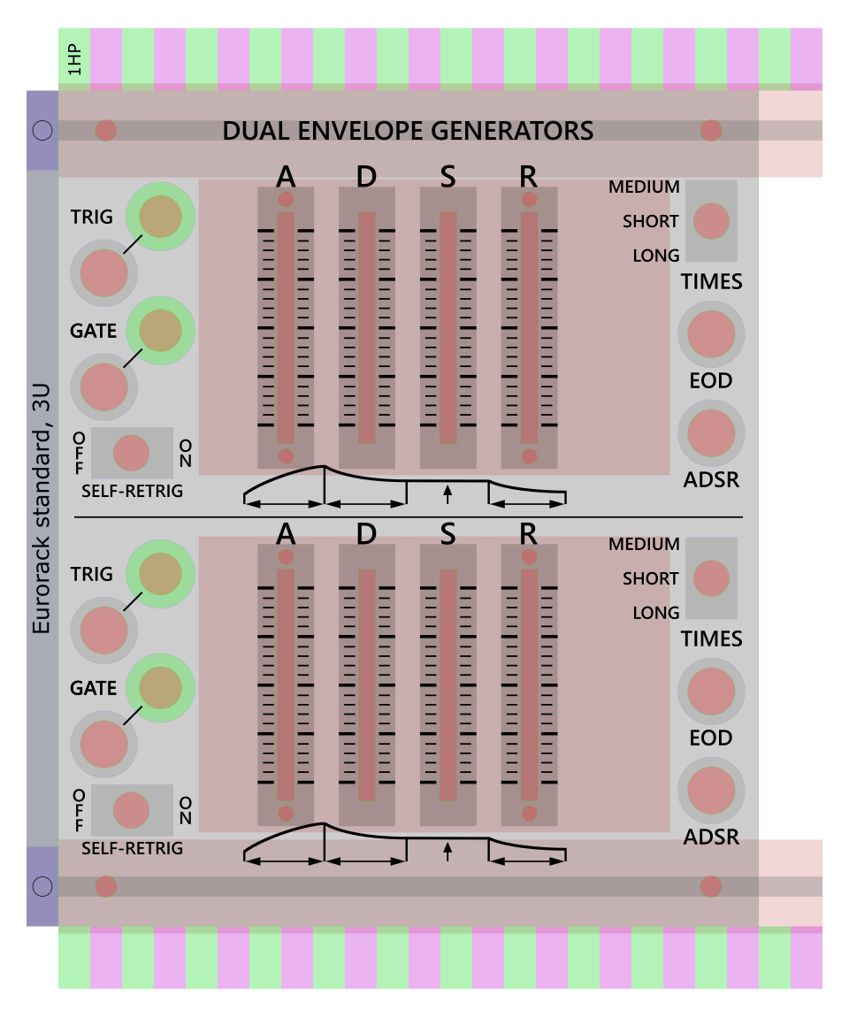
ADSR Envelope Generator Module
An Attack-Decay-Sustain-Release Envelope Generator (or ADSR EG for short) generates a voltage that changes over time, based on when a key is pressed and released, and some configurable parameters. It is used to shape parameters of the sound, creating a short plucky sound, a fading-in and out sound like you’d get from playing slow strings, or anything in between.
The ADSR EG module described in this article is based on the one designed by Ray Wilson of Music From Outer Space, but features some additions of my own. The MFOS article can be found here: ADSR Envelope Generator (+/-12V or +/-15V), or by going to the “Synth DIY” tab on the site and finding it in the sidebar on the left. Ray’s article has some nice detailed diagrams of the ADSR cycle in response to gate and trigger signals, too.

Contents
- Introduction
- Circuit description
- Additions to Ray’s circuit
- Changes for different power supplies / eurorack
- Components
- PCB
- Panel
- That’s it!
Introduction
Before we dive in, let’s get some terminology specific to this module out of the way. I’d also like to be clear about what additions I’ve made, so you can figure out if it’s of interest to you.
Be forewarned, this article goes rather in-depth about the working of most parts of the circuit. If you don’t need all the nitty gritty, you can always skip right to Circuit description > Circuit without additions to get to the overall explanation of the ADSR circuit before I added anything. Right after that section is the description of my additions.
Terminology / what ADSR does
- Gate:
The gate input is a logic signal, meaning it will be either off (0V) or on (5V). It is on if at least one key is currently pressed on the keyboard. When the last key is released, the gate returns to 0V immediately.
- Trigger:
The Trigger input is also a logic signal. This one is meant to be a pulse, meaning it goes from 0V ot 5V and right back again in about 1 millisecond. A trigger pulse is sent whenever a new key is pressed on the keyboard, including when one or more keys were already being pressed.
- Attack time, usually just “attack”:
The time it takes for the output of the envelope generator to rise from 0V to the maximum value. This starts when the gate input goes from low to high and/or when a trigger pulse is received.
- Decay time, usually just “decay”:
The time it takes for the output of the envelope generator to fall from the maximum value to the sustain value. Decay starts once attack has ended: when the envelope generator has reached the maximum output value.
- Sustain level:
The output voltage the envelope generator will stay at as long as a key is held, once the decay cycle has ended.
- Release time, usually just “release”:
The time it takes it takes for the output of the envelope generator to fall back to 0V, after releasing (all) keys on the keyboard. That is, once the gate input returns to 0V. Entering the release stage can happen at any time, during any stage, as it only depends on the gate input returning to 0V. The envelope generator’s output voltage will fall to 0V from where it was at at that time.

Picture adapted from ADSR_parameter.svg by Abdull on Wikipedia.
Additions in this version
The main addition are LEDs indicating the active stage of the ADSR cycle, but here’s a full list:
- Manual trigger button in addition to the manual gate button
- LEDs indicate the active stage of the cycle (through LEDS in the slide pot lever)
- Switch to self-retrigger once the decay stage has ended
- “End of Decay” (EOD) output, which produces a pulse
- An additional time selection, so instead of long/short times, the options are long/medium/short
Important note about supply voltage
My modular system runs on ± 5V, which is fairly unconventional.
As a result of this, some of my component values, mainly resistors, had to change to make that work. In this particular module, I also had to swap out regular opamps with rail-to-rail opamps, to ensure high enough output levels going into some logic level inputs. Consider this a warning that the circuit as presented below will likely not work with your existing synth power supply. In the section “Changes for different power supplies / eurorack” I go into detail about the changes needed.
Circuit description
I initially built this rather sloppily on breadboard, and blamed several glitches I was experiencing on bad connections on the breadboard. Leaving it like that, I drew up the schematic and a PCB, and sent it off to be fabricated. After painstakingly putting it together I found the thing was a total loss, as all the glitches I initally found were still there. Suffice to say I learned a valuable lesson about due diligence.
For revision 2, I took the time to properly understand how Ray’s original version works, allowing me to debug all the glitches that came up, before carrying on with my own additions. Since I learned a lot by doing that, I’d like to explain the circuit in depth—with all due respect to Ray Wilson’s explanation. Perhaps it’ll end up helping someone.
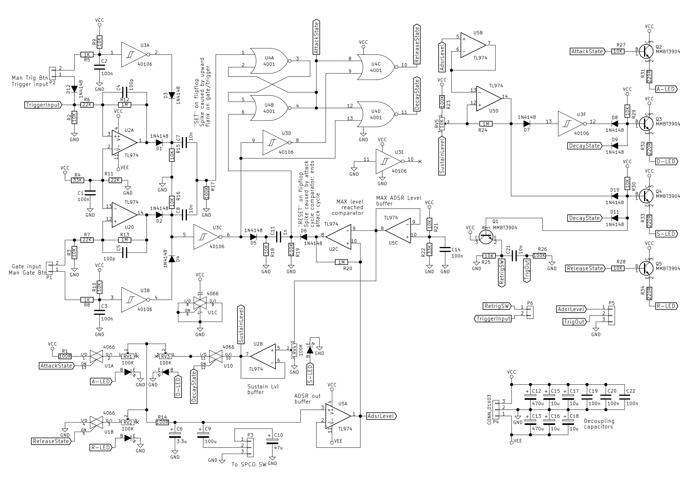
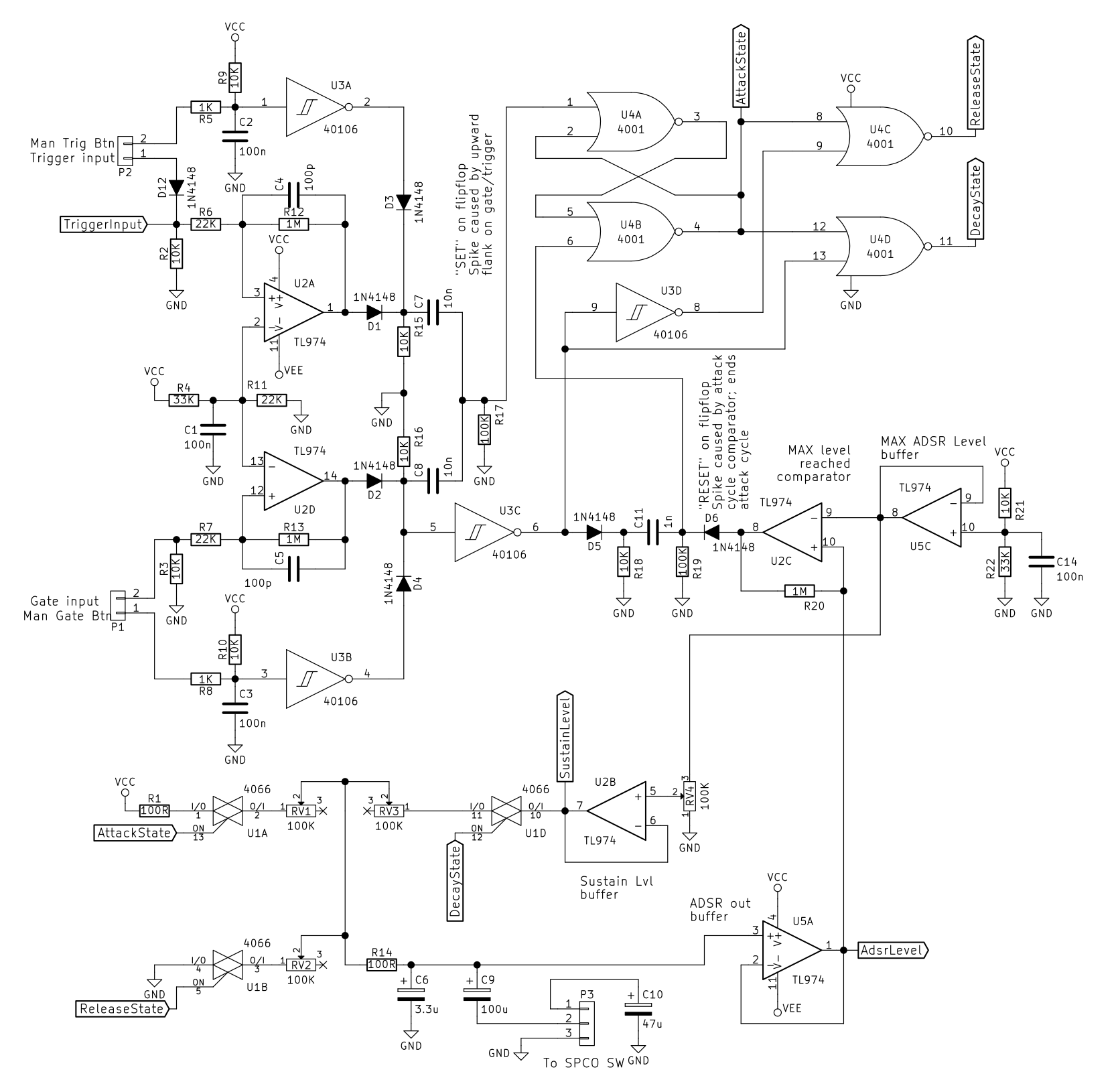
Gate and trigger inputs
The gate and trigger input signals are expected to be logic level signals, meaning they should be either 0V or 5V. We want to ensure a few things:
- Don’t draw more current than absolutely needed.
- Create a clean flank between on and off states, as any jitter when switching could cause our circuit to execute its timing functions multiple times in a row rapidly; this is essentially debouncing.
- Ensure we don’t send a signal out on the inputs. This only applies to the trigger, which I’ll elaborate on.
In this configuration, the opamps are used as voltage comparators. If the voltage on the non-inverting (+) input is higher than the voltage on the inverting input (-), the output of the opamp will be at its positive rail voltage, Vcc. In my case, this is +5V. If the voltage at the non-inverting input is lower than the voltage on the inverting input, the output will be at the negative rail voltage, Vee. In my case, that is -5V.
The diodes at the output of the opamps only allow current to pass if the voltage at the anode (left side) is higher than at the cathode. As a result, the voltage at the cathode will be either 0V or 5V. The cathodes of D1 and D2 carry logic signals “trigger on” and “gate on”.
R4 and R11 (in the middle) form a voltage divider. The voltage going into the inverting inputs of both opamps can be calculated as follows:
Vdiv = [ R11 ÷ ( R4 + R11 ) ] × Vcc → [ 22k ÷ ( 33k + 22k ) ] × 5V = 2V
Meaning that if the gate or trigger input voltage exceeds 2V, the output of the comparator will be high (5V), otherwise it will be low (-5V).
Capacitor C1 is added as a bypass capacitor, ensuring the voltage reference is stable at that voltage. If this capacitor were not present, any small current being drawn would throw off the resistor ratio, thereby affecting the voltage. You can visualize current being drawn as a resistor in parallel with R11. In the equation above, you’d have to substitue R11’s 22k with the parallel resistance, which will always be lower. As a result, the voltage would be lower.
Hysteresis
If the input voltage switches between low and high slowly, noise superimposed on the signal could cause the comparator to switch between high and low multiple times before settling on the intended state. Thanks to opamps’ very high “open loop” gain (voltage gain when there is no feedback path), all that’s needed to flip the comparator state is a voltage difference in the order of microvolts. In theory this is open loop gain is infinite, so, still in theory, you need only an infinitely small difference to flip the state.
To combat this, positive feedback is added, to make the comparator essentially “want to” stick to its current state, requiring a larger input voltage change in the other direction to get back to the other state. This is called hysteresis.
R12 and R13 provide positive feedback for each of their opamps. When the opamp’s output is high, some of that positive voltage is fed back to its non-inverting input (+), thereby raising the input voltage an additional bit over the reference voltage. Because the input voltage is now even further up from the reference voltage, any noise on the input is much less likely to push it down below the reference voltage again. The opposite is also true: when the input voltage falls below the reference voltage, the comparator will have -5V at its output, which is partially fed back to the input. In turn, the input voltage is moved a bit lower than it already was, again, away from the reference voltage.
We can calculate the change in voltage needed in either direction. When having flipped the opamp’s output in one direction, the input voltage will have to change this amount in the other direction to flip it back the other direction. R7 and R13 form a voltage divider, which let us calculate the feedback fraction, that is, the fraction of the output voltage that is added onto the input through the feedback resistor. We’ll use ‘B’ to refer this fraction:
B = R7 ÷ ( R7 + R13 ) → 22k ÷ ( 22k + 1000k ) ≅ 0.0215
Let’s define some variables before continuing:
- Vin(+) is the voltage measured at the non-inverting input of the opamp
- Vin(R) is the voltage measured at the left end of the resistor, in this case R7, it is where the signal comes in from outside this circuit.
- Vsat is the saturation voltage at the output of the opamp. In our case either -5V or +5V.
If we multiply the feedback fraction with the saturation voltage, we get what’s added to the value that was already at the input. The saturation voltage is the output voltage of the opamp, which will be one of the rail voltages when in saturation. This produces this formula:
Vin(+) = Vin(R) + B × Vsat
Let’s assume some initial conditions for an example. Our Vin(R) is at 0V, and the gate comparator opamp’s output voltage (Vsat) is saturated at -5V. Due to the positive feedback path, we can calculate that the actual voltage at the noninverting input becomes:
Vin(+) = 0V + 0.0215 × -5V = -0.1075V
This negative voltage gets added to Vin(R) to get Vin(+). We’ll see that the earlier explanation of having to pass 2V is, as a result, not entirely accurate.
Suppose now that Vin(R) rises to exactly 2V. Vin(+) then becomes 2V + (-0.1075V), or 1.8925V. This is below the 2V reference voltage, and as such, will not flip the comparator into positive saturation.
Once Vin(R) rises to slightly over 2.1075V, Vin(+) exceeds the 2V at the inverting input, and the opamp switches to positive saturation, producing +5V at its output.
For the sake of example, let’s keep Vin(R) at 2.1075V. Now that the comparator is in positive saturation, Vin(+) becomes:
Vin(+) = Vin(R) + B × Vsat → 2.1075 + 0.0251 × 5V = 2.2330V
If we now want to go back into negative saturation, Vin(R) will have to fall below 1.8925V, because 0.1075V is added to Vin(R).
As a result, to move between positive and negative saturation, we need a change of 2.2330V - 1.8925V or 0.3405V. You’d need some terribly noisy conditions to get that to happen uninentionally!
Finally, there are those capacitors C4 and C5. I have to admit I don’t actually know what they are for. I couldn’t find anything relating to hysteresis that advocated the addition of those. They are in Ray’s schematic and I took them into mine without giving them much thought. My best explanation I can come up with is that they’re a force of habit from other common circuit elements where they do serve a function.
Resistors to ground
R2, R3, R15, and R16 are all 10K resistors to ground. These ensure a voltage of 0V at their other end when no voltage is otherwise supplied to that point of the circuit. For instance, if nothing is connected to the gate input, that point would have an “undefined” voltage, which could lead to erratic, unexplained behavior. Tying it to ground through a resistor ensures it’s simply at 0V instead. If the non-ground end of the resistor is unconnected, no current flows through the resistor, leading to a voltage of 0V across it. If a voltage is supplied, a small current through the resistor will mean there is a voltage across it.
Diode at trigger input
A final detail of this portion of the circuit is the diode D12 at the trigger input. Later on, we’ll see how there is end-of-decay auto retrigger functionality in the circuit. This trigger pulse is fed back to the trigger input. The diode ensures this pulse is not also fed back to what’s connected to the input, when the voltage there is at 0V. Otherwise the input would also sort of act as an output, unintentionally affecting other modules.
Manual gate and trigger button inputs

The inputs for “manual gate” and “manual trigger” are meant to be connected to normally-open push buttons, of which the other end is connected to ground.
Schmitt triggers inverters U3A and U3B’s inputs are held high by the R9/C2 and R10/C3 combinations. Once a button is pressed, the open end of the 1K resistor (R5 and R8) is connected to ground. R9 and R5, and R10 and R8 then form voltage dividers, bringing the voltage at the inverter’s input down to 0.5V (given Vcc of 5V). This is close enough to 0V for a logic “0”.
A Schmitt trigger achieves the same thing as the hysteresis circuit described earlier; it will only toggle between high and low outputs if the difference in input voltage is great enough, thereby preventing oscillation at the tripping point.
The dashed lines indicate where this part of the circuitry connects to the previous piece shown. Diodes D3 and D4 ensure that a high voltage from that other circuitry doesn’t make it through to the output of the schmitt triggers while those are low.
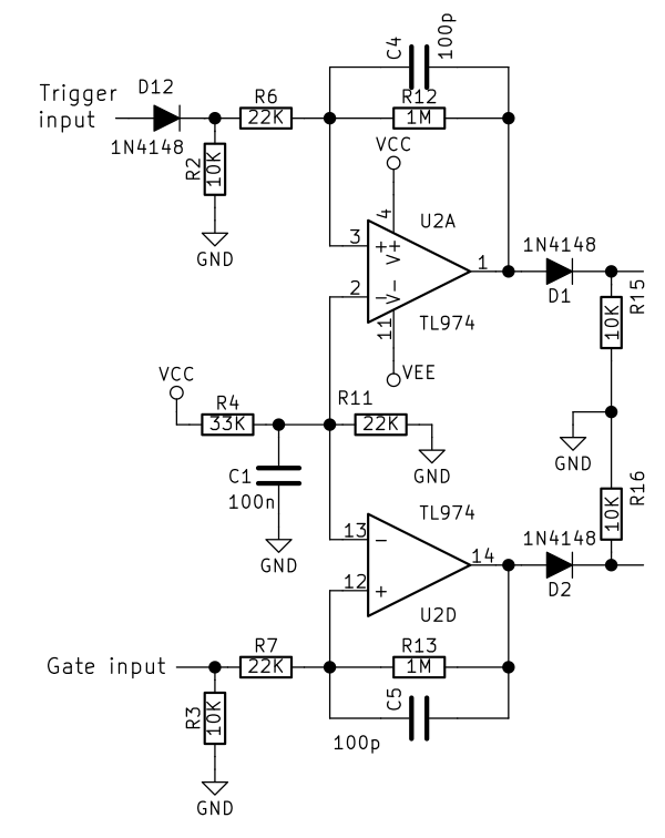
Rising flank to pulse converter
This little circuit can have many applications; it is used a few times in the ADSR. Further in the circuit, there is a standard set/reset flipflop comprised of two NOR gates. We will see there that we don’t ever want to have a logic “1” at both the SET and the RESET inputs at the same time. To accomplish this, we instead only use the minimum we need to operate the flipflop: a brief pulse at the appropriate input.
This small circuit accomplishes just that. I have to admit it took me quite a while to figure that this is how it was meant to behave when analyzing Ray’s circuit and debugging my breadboarded version.
The diodes D1 and D2 here are shown for reference to where you can find this bit in the larger circuit. This bit shows two flank-to-pulse converters combined into one output.
Let’s define our initial conditions as follows: Capacitors C7 and C8 are discharged, and the voltage at D1 and D2 is 0V. Now, when the the voltage at D1 suddenly becomes 5V, this voltage will appear across R15, as well as the series network of C7 and R17. Because C7 is at this point not charged at all yet, the voltage across it is 0V. Since C7 is in series with R17 and the voltage across both of them is 5V, that brings the full 5V across R17.
So, at this point our full 5V is available at the output of this little circuit. However, C7 will immediately begin charging, in the process accumulating more and more of the 5V across it. The more of the 5V is taken up by C7, the less remains across R17. Ultimately, it falls back to 0V very shortly after the flank from 0 to 5V.
Once the voltage at D1 returns to 0V, C7 quickly discharges again through R15.
The voltage across the capacitor over time can be calculated as:
Vc = Vin × [ 1 - e -t ÷ (R × C) ]
Where:
- Vc = voltage across capacitor
- Vin = input voltage, here voltage across C7 and R17 series network
- e = Euler’s number, a mathematical constant
- t = time in seconds
- R = series resistance in ohms (Ω) , in our case R17, 100 kΩ or 100,000 Ω
- C = capacitance in Farad, in our case C7, 10nF or 0.00000001 Farad
The voltage across R17 will be Vin - Vc.
R × C is also known as the time constant tau (τ). When multiplied you get a value in seconds. Given then above formula, it takes 5 × τ to charge a capacitor to 99.3% of Vin. 4 × τ gets you to 98.12%, 3 × τ to 94.93%, 2 × τ to 86.3%, and 1 × τ to 63%.
If you want to learn more about charge/discharge characteristics of capacitors, this learningaboutelectronics.com page seems like a good place to start: Capacitor Charging - Explained.
Anyhow, with those tidbits of formulas and pre-calculated ratios in hand, we can calculate our meaningful pulse length. The pulse output here will be used by logic ICs, namely the CD4001. A look at the datasheet reveals that the maximum input voltage to still be considered a logic “0” (VIL MAX) is some 2V.
Applying the 63% or 1 τ time constant R × C from earlier:
5V - 0.63 * 5V = 1.85V
So after 1 time constant we’re already more than in the clear. Let’s keep using that 1 tau constant though for ease of calculation. Our meaningful pulse duration therefore become approximately R × C without further ado. Filling in values from R17 and C7 this gives us:
100,000 Ω × 0.00000001 F = 0.001s or 1 millisecond.
Summarized: whenever we get an up-going flank from 0 to 5V at either D1 or D2, a 1ms long pulse appears at R17.
Note: to keep the above brief, I’ve neglected the 0.65-0.7V voltage drop across the diodes, and any small offset that might’ve been introduced by the opamp used. With the voltage a bit lower, it would mean that the resulting pulse duration is slightly shorter.
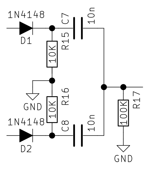
Max level reached comparator
In the circuit pictured, the current ADSR output voltage is connected to the line leading to the bottom (connecting to R20 and the non-inverting input of U2C). The line leading to the left edge of the image is the comparator output, which will be high when the maximum level is exceeded.
This part of the circuit establishes the maximum output voltage the ADSR cycle will reach. This level is reached when the attack cycle completes. Recall that that attack stage is when the voltage rises over a configurable time to the maximum level. Once it reaches this level, the attack stage is over and the decay stage begins..
We’ll work through this one from right to left.
Max ADSR level reference
Resistors R21 and R22 form a voltage divider (like we encountered earlier), stabilised by decoupling capacitor C14.
Given that Vcc is 5V, we can calculate that the reference voltage sits at [ 33K ÷ ( 10k + 33k ) ] × 5V = 3.84V
This reference voltage is buffered through a voltage follower comprised of opamp U5C. This simplistic opamp circuit ensures virtually no current is drawn from the actual voltage reference. Drawing current from a voltage divider would alter its voltage (because essentially you’d be putting a resistor in parallel with R22), defeating its purpose. Capacitor C14 also helps alleviate that problem. You can read more about voltage followers on learningaboutelectronics.com: What is a Voltage Follower?
Level comparator
The voltage reference is connected to the inverting input of U2C, while the ADSR output voltage is connected to the non-inverting input. If the reference voltage is higher than the ADSR output voltage, U2C’s output will be at the negative rail voltage (-5V). The other way around, once the ADSR output voltage exceeds the reference voltage, the output will swing to the positive rail (+5V).
R20 provides a tiny bit of hysteresis as we’ve seen before. Since there’s no physical second resistor there though, the feedback fraction will be very small.
Not pictured is a diode blocking current flow when the output is negative; resulting in an output that’s either a logic 0V or 5V.
Set/Reset flipflop made of NOR gates

Moving on to the digital domain now, let’s have a look at the set-reset flipflop, made of NOR gates. As a quick rehash: an OR gate will output a logic 1 (5V) if one or more of its inputs is at a logic 1. Think: if this or that is 1, then I’ll output 1. A NOR gate does the same, but it inverts that output. As a result, a NOR gate will output a logic 0 (0V) if one or more of its inputs is at a logic 1. Only if all of a NOR gate’s inputs are at a logic 0 will its output be a logic 1.
For reference, let’s see some the truth table. In this table, A and B are the inputs of the gate, and OR and NOR indicate the resulting output for each of these gates.
| A | B | OR | NOR |
|---|---|---|---|
| 0 | 0 | 0 | 1 |
| 0 | 1 | 1 | 0 |
| 1 | 0 | 1 | 0 |
| 1 | 1 | 1 | 0 |
Flipflop
A flipflop circuit is the most basic digital memory circuit; it can hold on to 1 bit of data. Let’s see how the NOR circuit shown accomplishes that. Our initial condition is that the power is off, so we have 0V everywhere (at “Set”, at “Reset”, at Q, at inverted Q). Q is the output of the flipflop, indicating the value stored in it. Q with a line over the top of it is “inverted output”, as if you’d run Q through a NOT gate. Let’s now power on.
Looking at U4A, a NOR gate, when the power comes on: Both “Set” and the other input are at 0V, leading to an output of “1”. Next, this means that a “1” is fed into one of the inputs of U4B, rendering its output “0”.
You may at this point notice that there is absolutely no reason why U4B wouldn’t settle on an output of “1” first, leading to a “0” on the output Q. This is absolutely right, and thankfully Ray Wilson thought of that. Circuitry external to this piece ensures that upon powering up, a short “1” pulse will be delivered to the “Reset” pin. This ensures that U4B will indeed be the one that outputs “0” on power-up.
Setting
After powering up, we have Q at “0”, inverted Q at “1”, and both “Set” and “Reset” at “0”. In this mode, the flipflop maintains its state. You can verify this for yourself by tracing those values back to the truth table for the NOR gate.
Now, when we supply a “1” to the “Set” input while keeping “Reset” at “0”, U4A receives at least one “1” on its inputs, turning its output (inverted Q)to “0”. With the previous “1” removed from U4B’s’ input, its output (Q) turns to “1” and the state maintains itself.
When you now remove the “1” from “Set” again, bringing both “Set” and “Reset” back to “0”, you can once again trace through and see the state being maintained.
Turning “Set” back to “1” at this point makes no difference, since one input of U4A was already at “1”.
Resetting
After setting, we have Q at “1”, inverted Q at “0”, and bot “Set” and “Reset” at “0”.
Now when we supply a “1” to the “Reset input” while keeping “Set” at “0”, U4B receives at least one “1” on its inputs, turning its output (Q) to “0”. With the previous “1” removed from U4A’s input, its output (inverted Q) turns to “1”. and the state maintains itself.
When you now remove the “1” from Reset again, bringing both “Set” and “Reset” back to “0”, you can once again trace through and see the state being maintained.
Turning “Reset” back to “1” at this point makes no difference, since one input of U4B was already at “1”.
Déjà vu? That’s normal, as resetting is exactly the same thing as setting, except the gates and outputs are switched around.
Flipflop truth table
This table is a bit different since it has to take into account the previous state of Q. We’ll use “old Q” for the state Q was in before the inputs “Set” and “Reset” are applied and “new Q” for the state Q will be in after applying.
Note: inverted Q is not listed in here, since it will always be the opposite of Q.
| Set | Reset | old Q | new Q |
|---|---|---|---|
| 0 | 0 | 0 | 0 |
| 0 | 0 | 1 | 1 |
| 0 | 1 | 0 | 0 |
| 0 | 1 | 1 | 0 |
| 1 | 0 | 0 | 1 |
| 1 | 0 | 1 | 1 |
| 1 | 1 | 0 | undefined |
| 1 | 1 | 1 | undefined |
Undefined here means that there’s no way of telling what the output will actually be. You can try to trace it through on the schematic, and you’ll find that with both “Set” and “Reset” high, the circuit perpetually wants to change the outputs. Summarised: don’t supply a “1” to “Set” and “Reset” at the same time.
We can rewrite this truth table to condense it a little bit, as it is often done in datasheets. In the following table, an “X” signifies that the his parameter makes no difference in determining the output. “old Q” as a value in the “new Q” column means that the value of Q remains unchanged.
| Set | Reset | old Q | new Q | Note |
|---|---|---|---|---|
| 0 | 0 | old Q | Memorize | |
| 0 | 1 | X | 0 | Reset |
| 1 | 0 | X | 1 | Set |
| 1 | 1 | X | undefined | Don’t. |
Use in the ADSR
Now that we’ve gone through the nitty gritty of how the NOR-gate based SR-Flipflop works, what is its actual use in this enveloper generator circuit?
The “Set” input of the flipflop connects to output of the gate/trigger’s flank-to-pulse converter circuit. In effect, whenever one of the following happens, the flipflop will be set to output “1”:
- The “Gate” input of the circuit goes from 0V to a logic high
- The “Trigger” input of the circuit receives a pulse
As you may recall, these are the conditions for starting the “attack” stage of the ADSR. The logic output of this flipflop says “attack state is active” when it is “1”.
The “Reset” input of the flipflop is connected to the “Max level reached” comparator we saw earlier. Once that maximum level is reached, this comparator goes to +5V, which makes its way to the “Reset” input, thereby ending the “attack” stage.
In the full circuit, you will also find an inverter U3C connected to the cleaned up “Gate” signal. This inverter is, among other things we’ll get to, connected to another rising-flank-to-pulse converter comprised of R18, C11, and R19, at which point it connects to the “Reset” input.
When the Gate signal falls from 1 to 0, inverter U3C’s output goes to “1” (a rising flank), generating this “reset” pulse. In this manner, losing the “Gate” signal also leads to resetting the flipflop, ending the “attack” stage.
Switching and timing circuit
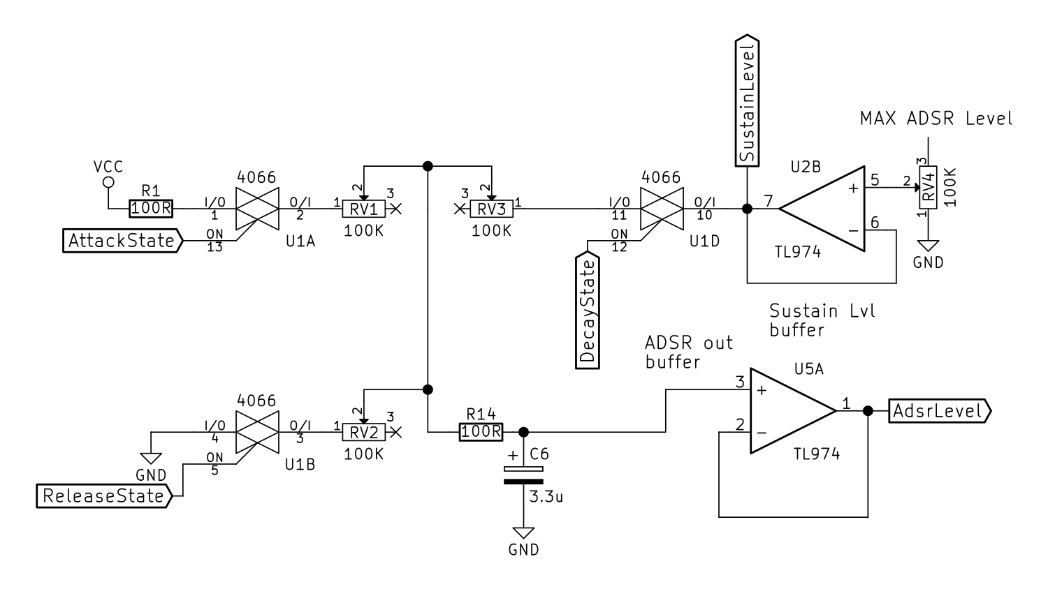
The bottom portion of circuit is what makes the actual envelope curve output happen. Everything is based around the timed charging and discharging of C6, through various paths. The CD4066 (U1), contains 4 “analog switches”. These are circuits that allow current to pass through in either direction (much like a mechanical switch), and they are controlled with a logic “0” or “1”, where the latter means the switch conducts current.
Also in the current path are the main potentiometers that determine the timing of the “Attack”, “Decay” and “Release” cycles. The “X” markings indicate an unconnected end of a potentiometer. In effect, these potentiometers are used as variable resistors, nothing any more fancy. In many circuits you’ll see this unused side connected the wiper (the arrow bit of the symbol), but in this case it was not practical for the PCB design to connect them.
There is one odd potentiometer in the circuit, namely RV4, which sets the sustain level. This one does not control timing, but rather sets the level for the “Sustain” stage, that is, what voltage C6 will discharge to in the “Decay” stage. The sustain level is a fraction of the “MAX ADSR level” which was discussed earlier, and isn’t pictured in this circuit. U2B buffers this voltage.
Finally, U5A buffers the voltage across capacitor C6, providing the main output of the entire circuit. This buffer ensures that anything using this output level doesn’t affect C6’s voltage level by drawing current from it directly.
How the cycle works
We have 3 important logic input signals in this portion of the circuit: “AttackState”, “DecayState”, and “ReleaseState”. Each of these will carry a logic “1” when we’re in the relevant stage of the cycle. There should never be more than one of these at a logic “1” at a time.
When the circuit just starts up, “ReleaseState” will be “1”, the other two “0”. With “AttackState” at “0”, U1A is open, so no current can flow from VCC to C6. “DecayState” is also “0”, so no current can flow from C6 to the sustain level buffer or vice versa through U1D. “ReleaseState” is “1” however, so U1B acts like a closed switch, providing a path to GND from C6. If there was any charge left in C6, it would at this stage drain to GND through R14 → RV2 → U1B; → GND.
At this point we’ll assume there is 0V across C6.
Attack state
Once we enter the attack state, “AttackState” is the only one that’s “1”. U1A is closed, so we have a current path from Vcc → R1 → U1A → RV1 → R14 → C6. This charges the capacitor. The rate at which it charges is determined by the total series resistance (R1 + RV1 + R14) and the capacitance of C6. RV1 is variable from 0Ω to 100 kΩ. The higher this resistance, the longer C6 will take to charge.
Once we reach the max ADSR level, as seen earlier, the logic portion of the circuit will ensure we leave the attack state and enter the decay state.
Decay state
Entering the decay state “DecayState” is the only one that’s “1”. The path from Vcc through U1A is now cut off, and U1D closes instead. Assuming for a moment that the voltage at “SustainLevel” is 0V, we can consider this point equivalent to GND. This means we now have a current path from C6 → R14 → RV3 → U1D → “SustainLevel” / GND. Through this path, C6 will discharge back to 0V. The time this discharging takes depends on the total series resistance (R14 + RV3) and the capacitance of C6.
If the voltage at “SustainLevel” is more than 0V, C6 will only discharge down to that voltage. The time this takes will be identical though, as voltage is no factor in the charge/discharge equation.
Once C6 gets down to “SustainLevel”’s voltage, it will remain there, it sustains that level.
Note: Functionality I’ve added means we can at this point restart the cycle when a switch is turned on, but I’ll leave that out for now; it’s not relevant to this partical piece of the circuit.
Sustain state
You may have noticed there is no logic flag for the sustain state in this part of the circuit. This is normal, because the sustain state is reached by C6 having discharged to the sustain level. No switching is needed to get from decay to sustain level, so there is no logic signal for it.
However, in my modifications to the circuit, I wanted to indicate the sustain stage on an LEDs along with the other stages, so I made modifications to create a logic signal for it as well. This has no bearing on the working of the switching and timing circuit though, so it’s not shown here. I’ll elaborate on it further down.
Release state
Once the player releases all keys (Gate input goes to “0”), “ReleaseState” will once again be the only one that’s at “1”. The path to “SustainLevel” through U1D is once again cut off, and the one to GND through U1B opens up. At this stage, C6 discharges to GND through C6 → R14 → RV2 → U1B → GND. The total series resistance (R14 + RV2) and the capacitance of C6 determine how long this discharge takes.
And with that, the cycle is complete.
Time range switching
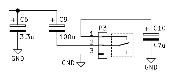
In the previous section I left out C9 and C10 for brevity, but let’s have a quick look at this now. With a switch connected to P3, we can switch between short, medium, and long ADSR timings by changing the total capacitance. The switch here needs to be one has 3 states: On-off-on.
In the middle state (off), the lever touches neither of the other endpoints, meaning that C9 ends up in an open circuit. In this state C6 is the only capacitor visible to the circuit, and the capacitance ends up as 3.3uF.
In the bottom state, the lever touches the bottom endpoint, which is connected to ground. This causes C9 to be in parallel with C6, producing a total capacitance of 3.3uF + 100uF or 103.3uF. This is the longest time range available.
In the top state, the lever touches the top endpoint, which is connected to C10. This results in the series network of C9 and C10 to be placed in parallel with C6. Series capacitance is calculated like parallel resistance: Cparallel = 1 ÷ [ ( 1 ÷ C9 ) + ( 1 ÷ C10 ) ]. For 100uF and 47uF this gives us 31.97uF or roughly 32uF. This, in parallel with 3.3uF, results in 35.3uF.
Summarizing, this setup lets us switch between 3.3uF, 35.3uF and 103.3uF to set the timing range.
Circuit without additions
Let’s now have an overview of the working of Ray’s entire circuit. In the below schematic, I’ve left out all of my own additions, save for the manual trigger and third timing capacitor. This section is mostly meant as an overview, and is a broader rehash of most of the parts we’ve already discussed.
Power-up
On power-up, the flipflop comprised of U4A and U4B will have its output “AttackState” initialized to a logic “0”, as we’ve seen earlier in the discussion of the flipflop.
With a logic 0 on the “Gate” input, the output of opamp U2D is negative, resulting in a logic “0” at the cathode end of D2. This “0” can then be traced through inverter U3C, so after that point it is a “1”. This “1” goes into NOR gate U4D. Having at least one “1” input (“AttackState” is “0”), its output is “0”. As a result, “DecayState” is initialized at “0”.
The “1” at inverter U3C’s output also makes its way through inverter U3D, supplying a “0” to one of the inputs of NOR U4C. “AttackState” is also “0”, so the output at U4C becomes “1”; “ReleaseState” is intialized to “1”.
Gate turns on
When the gate turns on, we get a “1” at the input of inverter U3C, which leads to a “0” going into inverter U3D, and, in turn, a “1” again into one of NOR gate U4C’s inputs. As a result, “ReleaseState” turns to “0”.
The positive flank from the gate signal creates a pulse at the “SET” input of the flipflop comprised of U4A and U4B, flipping its output “AttackState” to “1”. This same “1” is also fed to NOR gate U4D, ensuring “DecayState” remains at “0”. U4D’s bottom input is at “0” though now, as we have a “0” at the oputput of inverter U3C.
Attack state: capacitor charges, reached max level
We’re now in the attack state of the cycle. Analog switch U1A is therefore closed. Current flows from VCC to the capacitor network, however it is switched, gradually charging it and raising the voltage at “AdsrLevel”.
The voltage is compared to the constant “Max ADSR Level” at opamp U5C’s output. Comparator opamp U2C makes the comparison, though with a tiny bit of hysteresis provided by R20.
Once “AdsrLevel” goes beyond the max level, U2C swings to positive ouput. The logic “1” this creates at D6’s cathode is connected to the “RESET” input of the flipflop. So, once this goes high, the flipflop gets reset, and the “AttackState” goes back to “0”.
Decay state: capacitor discharges to sustain level
Now that “AttackState” is a logic “0” again, and “Gate” is still active, the inputs to NOR gate U4D are “0” (“AttackState”) and “0” (Gate’s “1” through inverter U3C). Only “0” inputs to a NOR gate makes a “1” output; “DecayState” is now at “1”.
Analog switch U1A, controlled by “AttackState” is now open, whereas analog switch U1D, controlled by “DecayState” is closed. The capacitor network now discharges down toward the voltage at opamp buffer U2B’s output voltage, namely the sustain voltage set by potentiometer RV4, where it remains once that is complete.
Release state: further discharge to 0V
When the player releases the last key, the Gate input returns to “0”. I’ve already discussed the circuitry that ensures this meanse we enter the release state earlier.
The capacitor network now discharges to ground through newly closed analog switch U1B (controlled by “ReleaseState”).
Release if we were still in attack state
A special case happens when the “Gate” input returns to “0” when “AttackState” is still active. The “1” → “0” transition at inverter U3C’s input leads to a positive flank at its output. R18, C11, and R19 form a positive flank to pulse converter as discussed earlier. This pulse goes into the “Reset” input of the flipflop, thereby ensuring the “AttackState” is indeed turned back off. The rest of the logic then follows just the way it was on power-up.
Retrigger through trigger input
When a pulse is retrieved at the “Trigger” input, this makes it throught to the “SET” input of the flipflop. This way, the attack state can be restarted when we had already reached “decay”, without having to first release the “Gate” input. This can be useful to keep a sound going at the sustain level, but repeating the initial pluck, or whatever attack/decay are set to.
Additions to Ray’s circuit
So far I’ve been describing just the part of the circuit as found on MFOS. Granted, I’ve re-drawn the schematic, but otherwise it it essentially the same thing. Before I undertook this project, I had seen Bourns’ PTL series potentiometers around online, and really wanted to do something with those. ADSR with LED state indication just seemed like great application for them, so that was my goal.
The circuitry to accomplish that also enabled a couple of handy extra features, which I’ll get to, but first I’ll focus on the new parts that allow us to drive these LEDs.
The way Ray’s circuit was laid out, my modification seemed straightforward: there are simple logic signals available indicating all the stages, so I just wire them up to a transistor driving an LED each, right? Almost. If you’ve been reading through all the earlier stuff you will have seen that Ray’s circuitry has no need for a “sustain” stage, so that’s one I had to come up with myself.
After I came up with the sustain stage signal, there was a further problem: I didn’t want the decay LED on when I’ve reached the sustain stage, so I needed further logic to only turn the decay LED on when in the decay state but not yet in the new sustain stage.
Anyway, let’s dive into how it’s done.
Transistor buffers
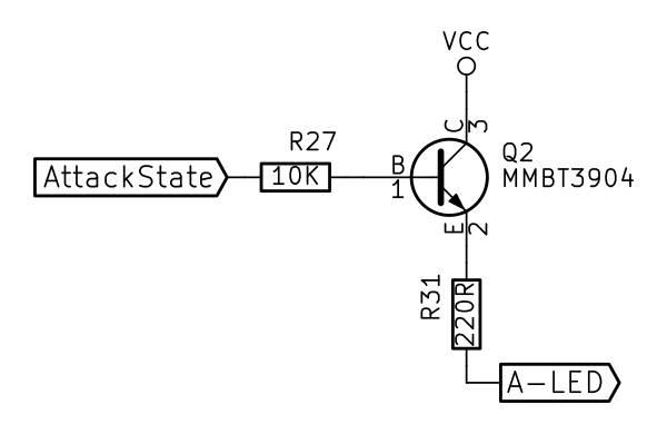
Each of the state LEDs is driven by a simple NPN transistor circuit, configured in a switching mode. This setup ensures that driving the LEDs does not draw much current from the generators of these logic signals. The LED needs a current of some 15mA for reasonable brightness, while these small signal opamps and logic gates are rated for only a few mA on their outputs. With the use of these 10K resistors going into the base, less then 0.5mA is being drawn from the logic sources for each LED.
The 220 Ω resistors are chosen as follows:
We know the forward voltage of the LEDs is about 1.8V, the supply voltage is 5V, and we want a current of roughly 15mA through the LEDs.
(5V - 1.8V) ÷ 0.0015 A = 213.33… Ω. The closest value in the E6 / E12 series is 220 Ω. This produces a current of 14.55mA, certainly close enough.
“SustainState” logic signal
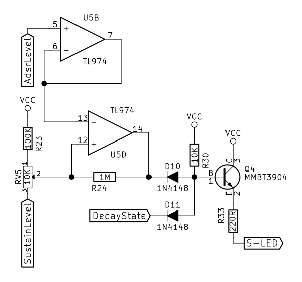
I defined the sustain state as “we are in decay state, and the output level is identical to the sustain level”. In practice, little more was needed to produce this signal.
Opamp U5B acts as an additional buffer (voltage follower) for the current ADSR output level, before using it in the comparator. The comparator U5D compares not directly to the sustain voltage, but to a voltage slightly above it. Trimpot RV5 lets you adjust just how much above it.
If the circuit did not use a voltage slightly above the sustain voltage, the Adsr output level would never be considered below the sustain voltage, as the capacitor network will only discharge to exactly that voltage. To make matters worse, at the ending stage of the capacitor discharging cycle, it takes exceedingly long to decrease in charge. So, by setting our comparison voltage to slightly above, we can ensure we always clearly get below this reference voltage. The trimpot allows tweaking just how long to wait until we consider the sustain level reached.
The hysteresis added by R24 is another reason the reference voltage should be a bit higher than the other voltage will actually reach.
Anyway, once the voltage at the negative input of U5D falls below this reference voltage based on “SustainLevel”, it will output 5V, or a logic “1”.
D10, D11, and R30 form a crude but effective AND gate. The point where they meet will only be at a logic “1” if both cathodes are at a “1”. If not, the point will be pulled down to GND, or logic “0”. I learned about some of these simple discrete gates on Hans Summer’s page on Discrete component logic. Keep in mind these can not be used in all circumstances.
This forms an AND between “sustain reached” and “DecayState”. We need “DecayState” in there, because otherwise our “SustainState” signal will be “1” during the attack state before the sustain level is reached, as well as in the release state. Clearly undesirable.
This logic signal is fed into the same kind of transistor buffer we saw before, and connected to the sustain level potentiometer’s built-in LED.
Decay LED logic
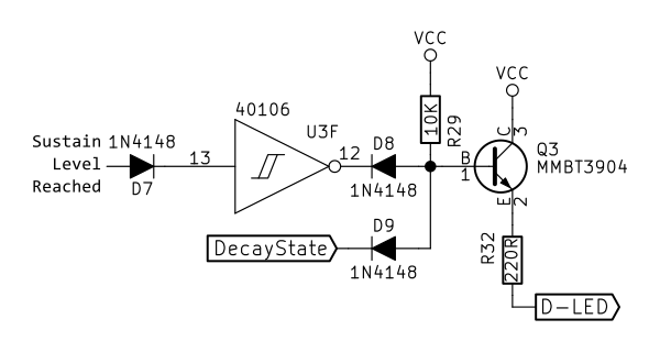
As previously mentioned, the other challenge was to only light the decay LED while we have not reached the newly defined sustain state yet. The renewed definition for decay state, only for the purpose of the LED, is: “we are in decay state AND we have not yet reached the sustain state”. This translates to logic gates without further ado.
“Sustain Level Reached on the left in the circuit is the output of comparator U5D we just saw. D7 ensures we don’t supply a negative voltage to inverter U3F’s input. U3F was an unused inverter from the 6 in the package, so I decided I might as well used that one rather than needlessly make a discrete transistor-based one. D8, D9, and R29 form another discrete AND gate.
Free features: auto-retrigger, end-of-decay pulse output
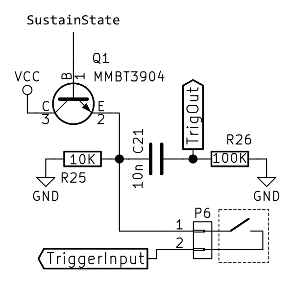
Having the new “SustainState” signal meant that I could add some other commonly found features. The rising flank from the “SustainState” signal can be fed back to the trigger input to automatically cycle the Attack and Decay stages, forming a sort of low frequency oscillator. This same trigger pulse can be output to trigger other modules like other envelope generators, allowing more complex modulation shapes to be created.
Auto-retrigger
Transistor Q1 buffers the “SustainState” logic signal. A switch connected to connector P6 optionally connects this signal back to the circuit’s trigger input. If this switch is closed, the circuit is retriggered the moment “SustainState” has been reached, and will enter the “AttackState” again. Since “DecayStage” is then no longer “1”, “SustainStage” immediately returns to “0”.
End-of-decay output
R25, C21, and R26 form another positive flank to pulse converter as we’ve seen earlier. This pulse signal is made available to other modules as an additional output on the panel.
That wraps up my additions to the Ray’s original circuit.
Changes for different power supplies / eurorack
As I’ve mentioned before, I have an unconventional setup, with my power supply at +/- 5V. Because of this, I’ve selected some component values that will most likely not work correctly in more regular systems like eurorack. In the following circuit diagram I’ve marked the areas of note that need adjusting for different supply voltages.
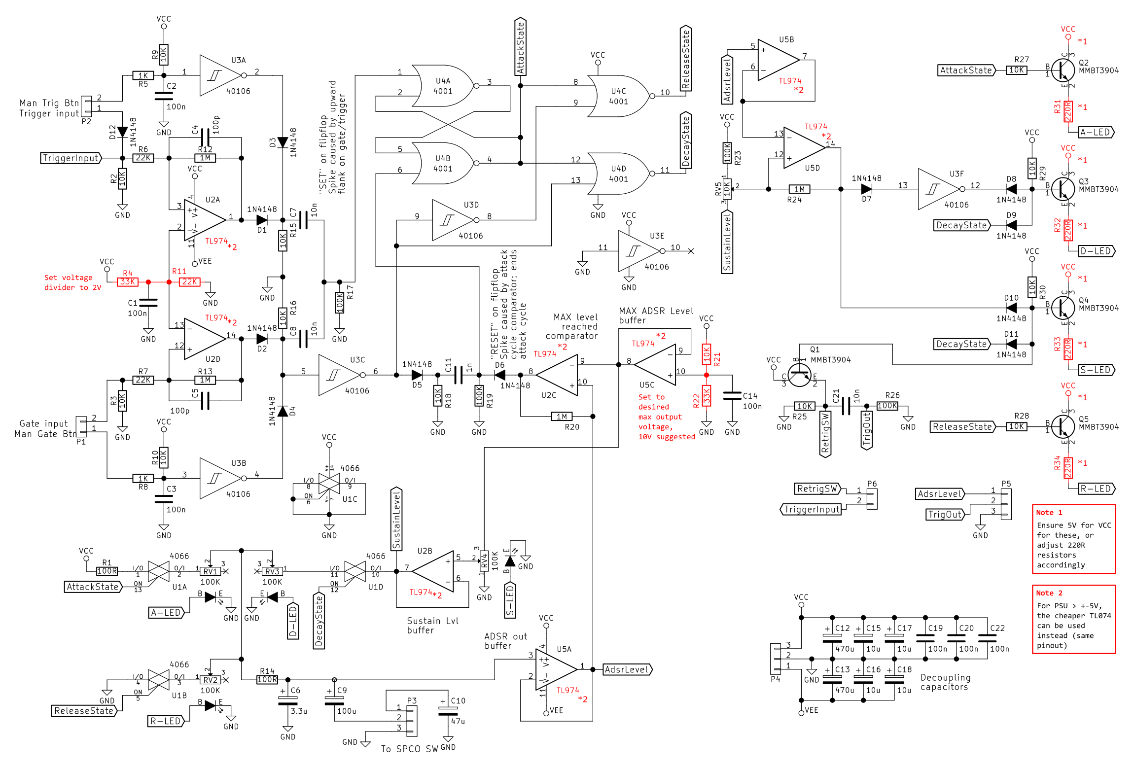
Gate / trigger comparator voltage
Opamp comparators U2A and U2D compare the input gate and trigger input signals to a threshold voltage of 2V. This value works well because it’ll do the trick even if you’re dealing with logic levels of 3.3V. Since these are logic level inputs (0V or 5V), you’ll want their reference voltage to remain at 2V. You can either replace the VCC connected to R4 with your 5V supply (if any), or recalculate R4 and R11 to set that voltage to 2V.
As a reminder, this reference voltage is set by the voltage divider formula:
Vref = [ R11 ÷ ( R4 + R11 ) ] × Vcc
Max ADSR output voltage
Another voltage divider is the one that sets the maximum output voltage of the envelope generator. This is the voltage that will be at the output when the attack cycle completes. R21 and R22 set this value based on Vcc. If you’re working with +/- 12V, you probably want to configure this voltage at 8-10V or something, depending on the usual control voltage range in your system. Doepfer’s A-100 system works with a max value of 8V for ADSR.
Again, the voltage divider formula:
Vref = [ R22 ÷ ( R21 + R22 ) ] × Vcc
Driving the LEDs
The resistors in the LED driving circuits are chosen for 5V. Either provide 5V to the collectors of these transistors (Q2, Q3, Q4, Q5), or change the values of the resistors at the emitters (R31, R32, R33, R34).
Recapping how to select resistors here, let’s define some parameters.
- Vcc: Positive power supply voltage, in my case 5V
- Vf: Forward voltage of the LED you’re using. For generic low power LEDs in red, green, yellow and orange, 2V is a good ballpark figure. Blue and white LEDs sit around 3.5V.
- Ic: Cathode current: the current you want through the LED. Typically you want this to be in the range 15-20mA unless you’re using high powered LEDs.
- R: Resistance of resistor in series with LED
Determine your resistance with the following formula:
R = (Vcc - Vf) ÷ Ic
Choice of opamps
I am using the TL974, which is a package of 4 rail-to-rail opamps. Regular opamps can only output to within a volt (or worse) from the opamp’s supply voltages. In this case this meant my opamps would only output a maximum of about 3.7 V, given my +/-5V supply. Since some of these opamps are meant to supply logic level signals (at 5V), this low output voltage, usually further decreased by 0.65V by a diode, didn’t cut it to get a clear logic “1”. To circumvent this issue, I used a rail-to-rail opamp instead, which gets to about 4.95V; close enough.
Long story short, if your supply voltage is higher than say, 7V, the TL074 will do the trick perfectly fine. It’s much cheaper as well. The pinout is identical, so it’s a simple drop-in replacement.
That’s all there is to change up!
Components
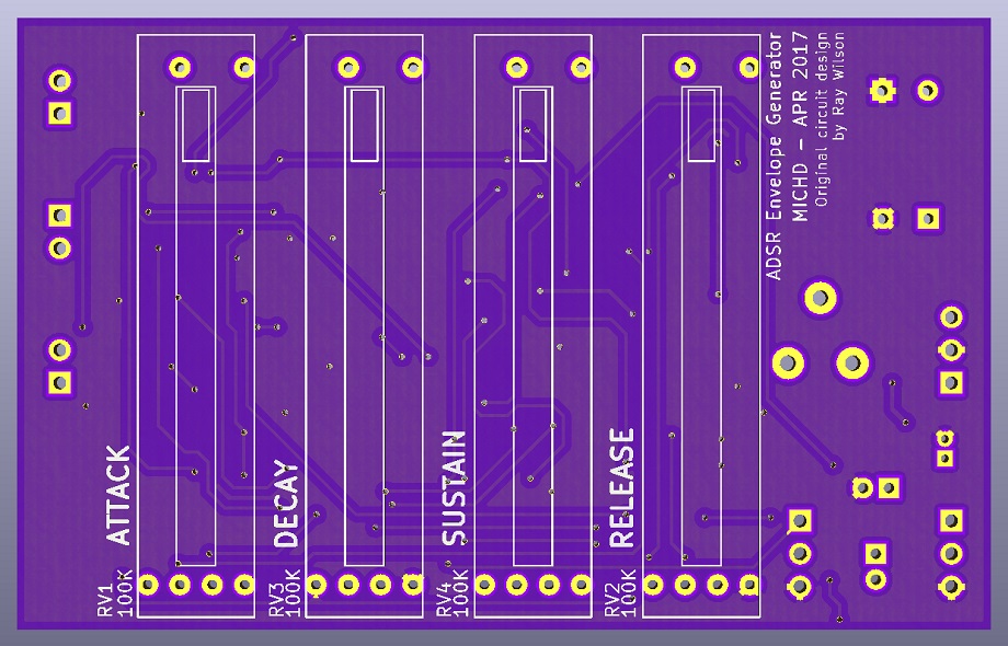
Slide potentiometer
I’m using Bourn’s PTL series linear slide potentiometers. They are regular slide potentiometers, except that they include an LED built into the lever. This makes them ideal to indicate the active state, associated with the parameter that slide pot controls.
Be sure to get a linear variant for this circuit. More info in the Bourns PTL series datasheet (PDF, 291 KB).
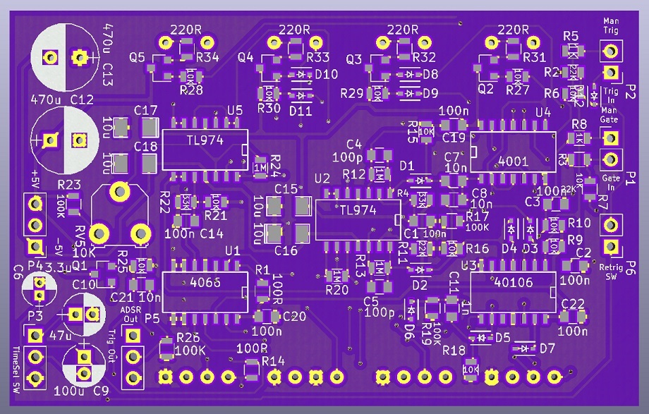
Full list of components
In this list of components, the bolded designators are the ones that are subject to change for different power supplies. (See above.)
| Qty. | Description | Value | Component designators |
|---|---|---|---|
| 13 | Resistor 1/8W 1%, 0805 footprint | 10 kΩ | R2, R3, R9, R10, R15, R16, R18, R21, R25, R27, R28, R29, R30 |
| 4 | Resistor 1/8W 1%, 0805 footprint | 1 MΩ | R12, R13, R20, R24 |
| 4 | Resistor 1/8W 1%, 0805 footprint | 100 kΩ | R17, R19, R23, R26 |
| 4 | Resistor 1/8W 1%, 0805 footprint | 220Ω | R31, R32, R33, R34 |
| 3 | Resistor 1/8W 1%, 0805 footprint | 22 kΩ | R6, R7, R11 |
| 2 | Resistor 1/8W 1%, 0805 footprint | 100 Ω | R1, R14 |
| 2 | Resistor 1/8W 1%, 0805 footprint | 33 kΩ | R4, R22 |
| 2 | Resistor 1/8W 1%, 0805 footprint | 1 kΩ | R5, R8 |
| 4 | Linear slide pot with LED, Bourns PTL30-15O0-104B2RV1 | 100 kΩ | RV2, RV3, RV4 |
| 1 | 6mm Trim pot (Triwood RM065 or similar) | 10 kΩ | RV5 |
| 7 | Capacitor, 0805 footprint | 100 nF | C1, C2, C3, C14, C19, C20, C22 |
| 4 | Capacitor, 0805 footprint | 10 uF | C15, C16, C17, C18 |
| 3 | Capacitor, 0805 footprint | 10 nF | C7, C8, C21 |
| 2 | Capacitor, 0805 footprint | 100 pF | C4, C5 |
| 2 | Electrolytic TH capacitor | 470 uF | C12, C13 |
| 1 | Electrolytic TH capacitor | 3.3 uF | C6 |
| 1 | Electrolytic TH capacitor | 100 uF | C9 |
| 1 | Electrolytic TH capacitor | 47 uF | C10 |
| 1 | Capacitor, 0805 footprint | 1nF | C11 |
| 12 | Small signal diode, SOD-323 footprint | 1N4148 or 1N914 | D1, D2, D3, D4, D5, D6, D7, D8, D9, D10, D11, D12 |
| 5 | General purpose NPN transistor | MMBT3904 | Q1, Q2, Q3, Q4, Q5 |
| 2 | Quad (rail to rail) Opamp | TL974 | U2, U5 |
| 1 | CMOS Quad bilateral switch | CD4066B | U1 |
| 1 | Hex Schmitt Trigger Inverter | CD40106B | U3 |
| 1 | Quad 2-input NOR Gate | CD4001 | U4 |
| 3 | Molex KK 254 2 pin connector | - | P1, P2, P6 |
| 3 | Molex KK 254 3 pin connector | - | P3, P4, P5 |
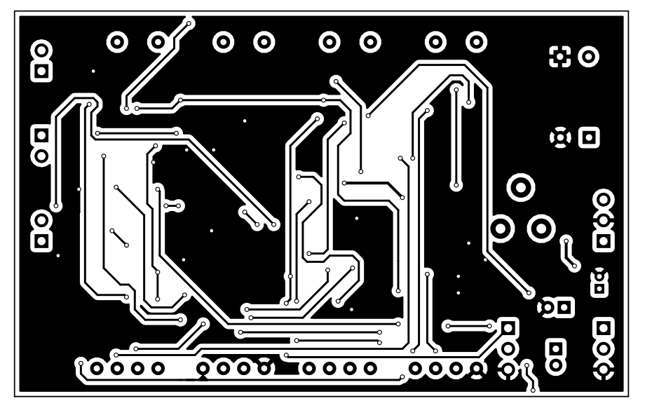
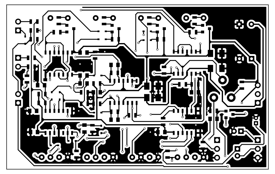
PCB
The PCB is a compact dual layer design, designed to fit two on a 3U panel. It was designed in Kicad, and you can find all the files on GitHub. You can also download the Kicad project for just this module as a ZIP file: adsr-eg-kicad.zip (74 KB).
Below are previews of both copper layers, as well as renders of the board. If you do decide to fabricate the board or have it fabricated by one of the numerous PCB fabrication places, you’ll want the kicad files though. I definitely recommend having them fabricated rather than doing this one at home. I had mine done by the good folks over at OSH Park.
Panel
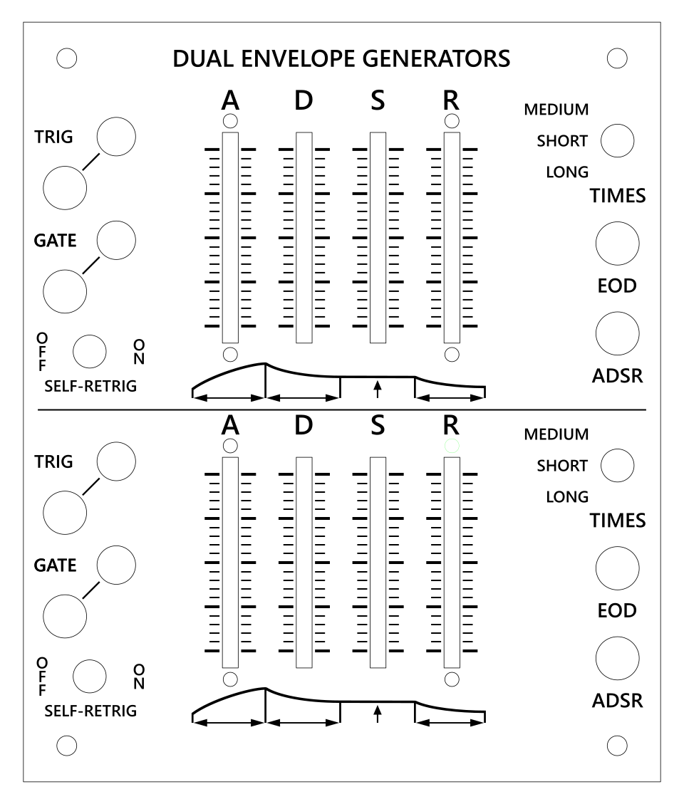
I make my front panels out of laser cut and engraved acrylic, using a laser cutter at my local makerspace (Southampton, UK’s SoMakeIt). For the design, I use the free and open source vector graphics editor, Inkscape. My system uses 3U dimensions, much like Eurorack. Because designing front panels is a repetitive task with recurring elements, I’ve made an SVG helper file that speeds up designing a new panel considerably.
Shown here is the panel the way it looked when I was doing the layout. I have a collection with common elements, corresponding to the switches, potentiometers, banana plug sockets, and so forth that I have laying around. I then copy these into my layout, and go to work aligning properly, labeling, and so on.
Large red-ish zones are “keep out” zones, meaning I can’t put any hardware in that area like potentiometers or switches because there’s something in the way. In this case it’s mainly the PCB that extends to the right of the actual slide pots quite a bit.
The laser cutter at the makerspace gives special meaning to certain vector graphic elements, namely:
- 0.01mm thick green stroke = cut
- full black fill = engrave
Colors can be further configured for function / engrave power and such, but for my panels, those are the only two I need. Similar settings can be used if you have your panel cut at a place like Ponoko.com (USA) or Razorlab.co.uk (UK).
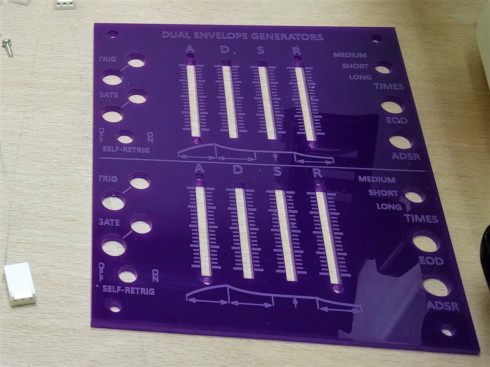
After I’m satisfied with the layout, I save a new version for lasering, and remove all the helpers, then ensure I’ve got the cutting width/color correct as mentioned before. I’ve shown the result of that here, though I’ve replaced the thin green cutting lines with thicker black lines, otherwise they would not be visible at all.
The linked SVG does have the right line widths and colors for cutting, however.
The acrylic I use for these front panels is Perspex cast acrylic, at 3mm thick. I buy it in A4-sized sheets from eBay. In the UK there generally are several sellers selling the stuff, so it’s readily available.
Laser cut jobs like these generally only take less than 10 minutes actual cutting / engraving time, engraving being the slowest part.
In all honesty, I’m now going to ramble on for a paragaph. The reason is simple: when viewed on a wide screen, the latest image stretches below this text, and I think that looks ugly. I don’t know what else I can say about it, so that’s why you’re reading this last paragraph before the photo of the finished, pre-assembly panel. Considering the amount of information in this article, I think I can get away with a single filler paragraph though, right? Well, this’ll do, thanks for your understanding.
That’s it!
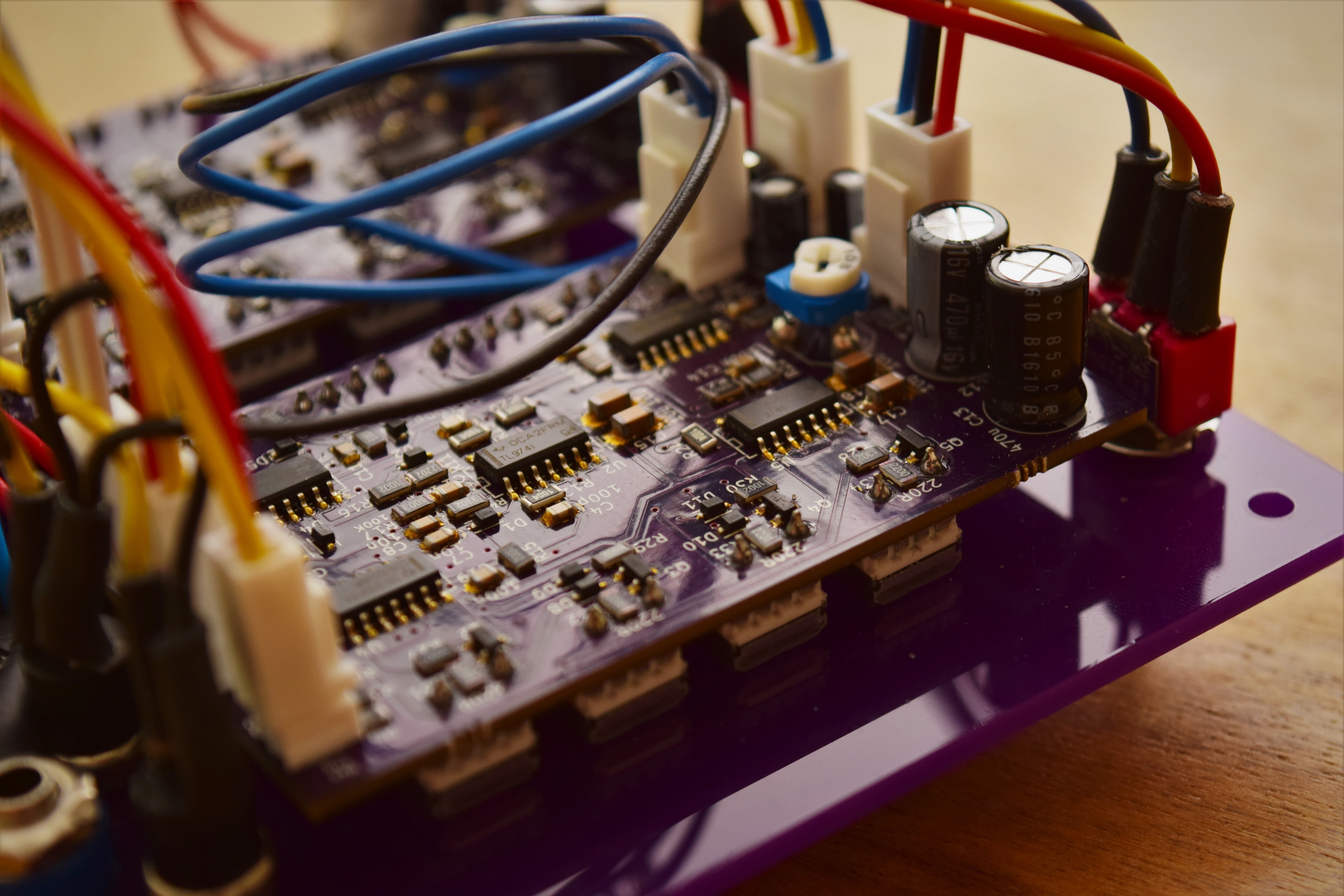
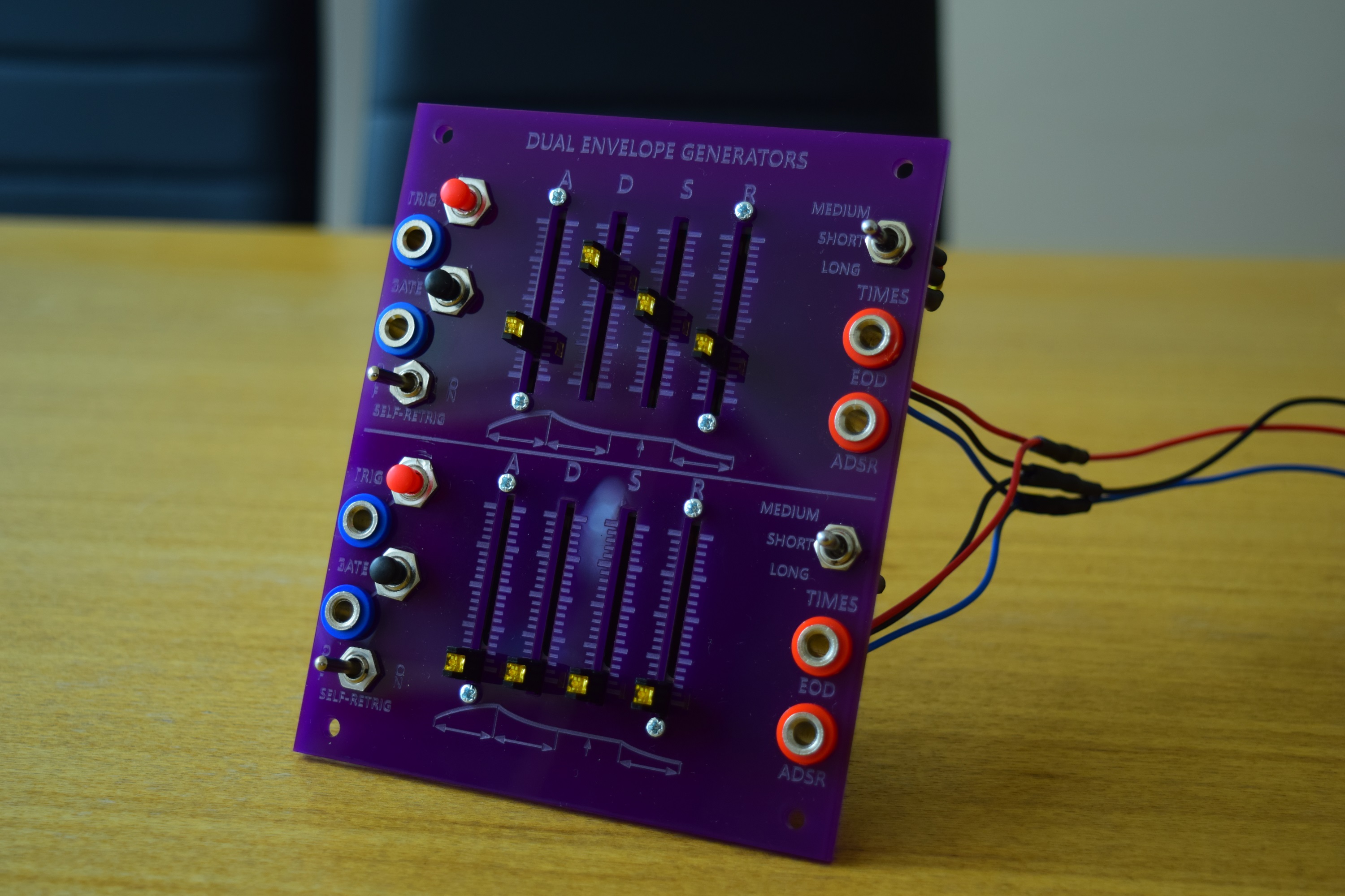
With the panel done, it’s a matter of wiring up the switches, buttons, and banana plug sockets, leading to the finished product:
You can also watch a Quick demo video over on Youtube, where I have one ADSR generator control filter cutoff, and the other amplitude.
I hope the article has been informative. You can send me feedback through Mastodon @MichDdev, where we can also find other ways for lengthier feedback. I regularly post pictures of my synth DIY stuff in progress on there too.